

Inside AI Chips, the Memory Interface Eats the Edge
On Nvidia's Rubin die, HBM4 controllers and PHY reportedly claim about 16% of the priciest silicon real estate.
BusinessThe expensive chip’s edge is being eaten up by an interface
Reader, let’s look down at an AI accelerator from above. In the middle sits the compute die, with HBM stacks pressed right up against it on either side. The compute die is built on the most advanced process node available, so every square millimeter of it is precious real estate. But the edge of that real estate isn’t doing computation — it’s occupied by an interface that exchanges signals with the neighboring HBM. That interface splits into two parts: a memory controller that manages when and where data gets read and written, and a PHY1 — the physical layer that actually pushes electrical signals off the chip.
There’s an estimate that shows just how large this interface has gotten. One semiconductor analysis report put the combined area of the HBM4 controller and PHY on Nvidia’s Rubin compute die at roughly 16%. That’s not a figure Nvidia has disclosed — it’s an outside estimate. Still, the direction is clear. A sizable share of the most expensive real estate on the most advanced process node is going not to computation, but to communication.
In this issue, I’ll use numbers from Samsung Electronics’s diagrams to show how much bigger this interface has grown generation over generation, and look at how custom HBM shrinks it. Then I’ll turn to NVHBM, which Nvidia unveiled in late August, and the question it raises about this whole shift.
The gateway widened with each generation
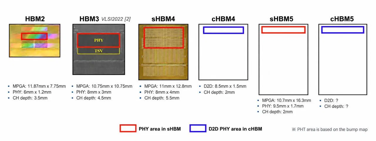
Samsung Electronics’ HBM generation comparison diagram lists the PHY size for each generation. Converting width × length into area gives us this:
| Category | PHY Size | Area (calculated) |
|---|---|---|
| HBM2 | 6mm × 1.2mm | ~7.2mm² |
| HBM3 | 8mm × 3mm | 24mm² |
| Standard HBM4 | 8mm × 4mm | 32mm² |
| Custom HBM4’s D2D interface | 8.5mm × 1.5mm | ~12.75mm² |
| Standard HBM5 | 9.5mm × 1.7mm | ~16.15mm² |
This diagram maps the area on the HBM die side where signals enter and exit, and according to the diagram’s annotations, it’s based on the bump layout. The gateway on the compute die side has to receive the same signal lines, so you can read these figures as an indicator of which direction both gateways’ sizes are moving.
From HBM2 to standard HBM4, PHY area grew more than fourfold. The main reason is the increase in the number of signal lines. According to Samsung Electronics, the data I/O pin count doubled from 1,024 to 2,048 with HBM4. Just as more lanes mean more tollbooths, more signal lines flowing in and out mean a wider gateway.
The numbers for custom HBM4 reverse this trend. Standard HBM4’s PHY measures 32mm², but the die-to-die (D2D)2 interface used by custom HBM4 comes in at around 12.75mm² — roughly a 60% reduction. Of the two dimensions, the longer one actually grew slightly, from 8mm to 8.5mm, while the shorter one shrank sharply, from 4mm to 1.5mm.
It’s also notable that standard HBM5’s PHY area is listed as smaller than standard HBM4’s. You could read this as the standard spec itself moving toward a narrower gateway, but since HBM5 is a generation whose products haven’t shipped yet, it’s too early to call it a trend based on a single figure. The D2D size for custom HBM5 is still marked with a question mark on the diagram.
 The Controller Moves Downstairs
Shrinking the number of channels doesn’t stop at swapping out the PHY. You can pull the memory controller itself out of the compute die and move it down to the bottom layer of the HBM stack — the base die3.
What made this possible was a process shift in the base die. Up through the previous generation, HBM base dies were made using DRAM process technology, but starting with HBM4, a path opened up to make them using logic process technology instead. Samsung Electronics has stated that its HBM4 uses a 4nm logic base die. Logic processes pack transistors more densely and offer more interconnect layers, so you can fit far more circuitry into the same area.
Once the controller moves down to the base die, all that’s left between the compute die and the HBM is a narrower, faster D2D connection instead of the standard HBM bus. The compute die gets back both the real estate the controller used to occupy and the broad footprint the PHY used to take up, and that space can now be filled with more compute units or cache. This matches the industry explanation laid out by Semiconductor Engineering, a trade publication focused on chip design. The idea is that the footprint the controller newly occupies on the base die is cheaper real estate than the footprint it frees up on the compute die. It’s the same circuit, relocated from the most expensive land to cheaper land.
Samsung Electronics goes a step further than this. According to Samsung’s own explanation, a base die carrying a custom HBM controller can also house spare resources for SRAM repair, status-monitoring functions, connections to external memory, and even the capability to handle some computation right beneath the DRAM itself. The picture that emerges is of the base die transforming from a signal-relay floor plate into a small logic chip in its own right.
So the payoff from custom HBM comes in two layers. There’s a performance-side effect — higher bandwidth per unit of interface area and simpler interposer4 wiring — and there’s a structural-side effect — the ability to re-plan how real estate is used on the compute die. It’s a technology for raising bandwidth, and at the same time, a technology for redrawing the floor plan of the accelerator itself.
Nvidia Showed Up First With a Blueprint
This shift moved from drafting-table talk to market reality on August 26th. Nvidia expanded its NVLink Fusion program and announced NVHBM.
NVHBM points in the same direction as the custom HBM we just looked at. Nvidia puts its own memory controller into the HBM base die and uses a narrower serial D2D connection instead of the standard bus. Nvidia claims up to a 30% increase in per-stack bandwidth, a 15% cut in HBM power consumption, and up to 25% more compute-die area, all compared to standard HBM4E. Reports citing Nvidia’s technical blog put the compute-die area gain as high as 30%, so the figures don’t quite line up. Either way, these are the company’s own claims, not values verified in an actual shipping product.
What caught my attention wasn’t the performance numbers but the division of labor. Until now, custom HBM has generally meant the memory maker and the customer co-designing the base die together. NVHBM flips that: Nvidia defines the controller and interface, and multiple memory companies supply and validate the same implementation. Nvidia explains that this cuts down the effort of integrating and validating memory from multiple suppliers. It also stated that NVHBM shares the same foundation as the technology Nvidia plans to use in its own GPUs going forward.
Who gets to use it is also fixed in advance. NVHBM is a component made available to NVLink Fusion partners, and the first named partner is Annapurna Labs, Amazon’s chip design organization. Annapurna said it will support NVLink Fusion starting with Trainium4. Nvidia’s blog, however, doesn’t explicitly state that NVHBM itself is built into Trainium4.
Samsung Electronics has also put out a timeline. It said HBM4E samples will ship to customers in the second half of 2026, with custom HBM samples following from 2027. So on the same foundational layer, a memory company’s custom design and Nvidia’s own implementation are set to reach the market at roughly the same time.
Oswarld’s Lens
What I notice in this news isn’t the bandwidth figures—it’s the question of who gets design authority over the base die. When the bottom layer of HBM was just a baseplate relaying signals, memory companies could design it however they pleased. But once that layer houses a controller and takes on part of the computation, it becomes part of the accelerator’s design.
If memory companies and customers co-design this layer, the memory company takes a step into the customer’s chip design. If the customer fixes the implementation and sources the same design from multiple suppliers, memory companies end up competing over who can build someone else’s blueprint better and in greater volume. In either case, memory companies’ revenue could grow, but where bargaining power accumulates looks quite different.

Closing
The technology that reclaims land on the compute chip ultimately comes down to laying new circuitry on the bottom layer of HBM. Who designs that layer’s circuitry determines whether the same technology becomes an opportunity for memory makers—or just another spec they have to follow. When custom HBM samples arrive in 2027, I’ll be watching the shape of the contracts as closely as the spec sheets.
💬 When you’re choosing or evaluating an AI chip, have you ever checked who actually controls the memory-side design? Let me know in the comments.
📨 If you have a colleague who follows the semiconductor supply chain, please share this piece with them.
Already a subscriber? Sign in to join the conversation


References & Further Reading
- Samsung Ships Industry-First Commercial HBM4 With Ultimate Performance for AI Computing (Samsung Newsroom)
- NVIDIA NVLink Fusion Expands With NVHBM Custom High-Bandwidth Memory (NVIDIA Blog)
- Nvidia unveils custom high-bandwidth memory (TechRadar)
- NVIDIA NVHBM Moves the Memory Controller Into the HBM Stack (StorageReview)
- Nvidia expands NVLink Fusion strategy to supercharge custom silicon memory (SDxCentral)
- How Will The Custom HBM Business Work? (Semiconductor Engineering)

📝 Glossary
Footnotes
-
PHY (Physical Layer): This is the circuitry inside a chip that sends and receives digital signals over the wires leading outside the chip. Paired with the controller that organizes the data, it forms the memory’s “gateway.” ↩
-
D2D (Die-to-Die) interface: A communication circuit that links chips sitting side by side within a single package over very short distances. Because signals don’t need to travel far, it can be built smaller than a standard memory PHY. ↩
-
Base die: The bottommost chip onto which HBM’s DRAM layers are stacked. It relays signals between the upper DRAM layers and the outside chip, and starting with HBM4, it’s made using logic process technology, allowing it to pack in more functionality. ↩
-
Interposer: An intermediate substrate that places the compute chip and HBM on a single board and densely wires them together. The more signal lines there are, the more complex this board’s wiring design becomes. ↩
Related issues
Dark Patterns: Do Users Search for the Law or Coupang?
Korea's FTC released new dark pattern guidelines, revealing a stark divide between what the law bans and what frustrates users.
BusinessThe Same EMF-Blocking Sticker Test, Run Four Times in 12 Years
Government notices say both 'it's safe' and 'reduce exposure' on the same page
BusinessMeta Releases Muse Spark Open, an 816B Open-Weight Model
Meta just open-sourced an 816-billion-parameter model that needs two Mac Studios to run at home.
Business
Your take shapes the next issue
What resonated most in this issue, or where has your experience been different?